Bloch Wave Algorithm
The PRISM Algorithm we have explored in the previous section used a planewave expansion to construct the exit wavefunction, by applying the multislice operator to each planewave. An alternative expansion, which can be very efficient for small periodic structures, is the Bloch wave formalism which uses Bloch's theorem to ensure basis functions respect the crystal periodicity explicitly:
where , , and are the Bloch wavevectors, reciprocal lattice vectors, and planewave coefficients respectively.
Bloch’s Theorem
Our starting point is once again the time-independent Schrödinger equation, (3.2):
where we have introduced the slowly-varying envelope function, , by separating the rapidly-oscillating component of the electron wavefunction according to:
To proceed, we expand both and as sums of Bloch waves:
which when substituted back into (7.2), result in an infinite set of coupled equations for the planewave coefficients .
1D Toy Example
Before we apply (7.4) to realistic potentials, it is instructive to consider a 1D toy example, which you might have come across in your quantum mechanics courses.
We will consider the following periodic potential with lattice constant :
where is the 1D reciprocal lattice vector. If we only include three reciprocal lattice vectors, , in our expansion we can write the coupled set of equations as:
The eigenvectors, , and eigenvalues, , may now be solved by diagonalizing (7.6) for each . Figure 7.1 plots the eigenvalues for in the first Brillouin zone, for different values of the potential.

VBox(children=(FloatSlider(value=0.0, description='potential strength, V$_0$', layout=Layout(height='30px', wi…Bloch Matrix Eigenvalue Problem
Now that we have built intuition with the toy 1D potential using a 3x3 matrix, we turn our attention back to the formal treatment, following De Graef, 2003, by inserting (7.4) into (7.2) to give:
which can be recasted as an eigenvalue equation:
where we have defined the eigenvalues, , and excitation error, , which describes how far a specific reciprocal lattice vector is from the exact Bragg condition, which in turns determines how strongly that beam is excited during electron diffraction.
Thickness effects are incorporated by propagating the wavefunction at depth according to:
The coefficients are chosen to satisfy the Bloch wave expansion of the Fourier components of the input wavefunction, , according to:
Selected Area Diffraction Patterns
As we saw above, planewave diffraction is at the heart of the Blochwave simulation method, so we will explore that first. All other types of measurements we will discuss can be constructed using individual planewave calculations.
Kinematical and Dynamical Diffraction
We consider our Si3N4 crystal, viewed along the [001] zone axis. The first step is to extract the parametrized scattering factors for each atom in our structure, and evaluate them on each of the structure’s reciprocal lattice vectors within a specified cutoff distance. We then use this to form the kinematical SAED patterns, by weighting the structure factor intensities with the reciprocal vector’s excitation error as we saw above.
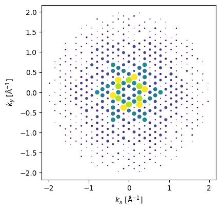
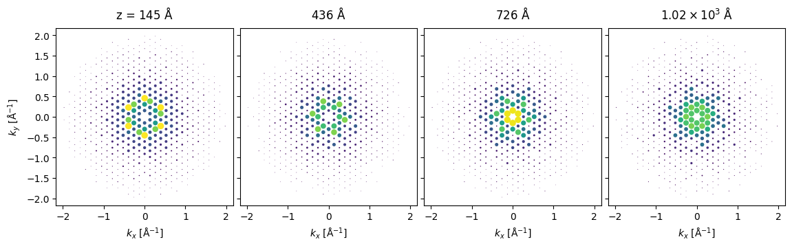
We can then use (7.9) to model dynamical scattering and plot the resulting SAED patterns as a function of thickness. Notice how, in addition to overall increased scattering, the modulation of intensities within the pattern changes with thickness.
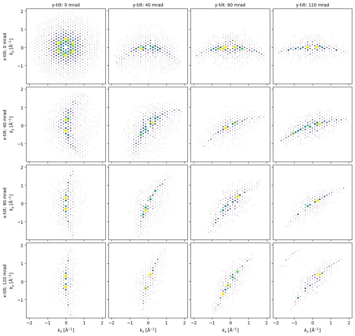
Tilted Crystal Electron Diffraction
One of the advantages of the Blochwave algorithm, as compared to multislice, is that scattering from arbitrary orientations of the structure is straightforward to calculate. Figure 7.4 illustrates this by calculating a 4x4 grid of dynamical SAED patterns, for different x- and y- crystal tilts. Notice how the Laue circle -- the ring of strongly excited reflections -- shifts around the pattern. Understanding how the Laue circle corresponds to crystal tilting is essential for successfully bringing a crystal onto a zone axis orientation.
Converged Beam Electron Diffraction
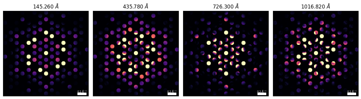
As we illustrated above, dynamical diffraction causes strong intensity oscillations between diffracted beams, which can be observed by tilting the crystal. This is typically done by capturing a CBED pattern -- where different angles within the probe’s numerical aperture correspond to tilted planewave illumination.
Since the excitation of the Bragg beams oscillates as a function of tilt with a period that relates to the crystal thickness, measuring CBED fringes can be used to estimate thickness. Figure 7.5 illustrates this effect by calculating CBED patterns for Si3N4 using a convergence angle of 5 mrad, for various crystal thicknesses.
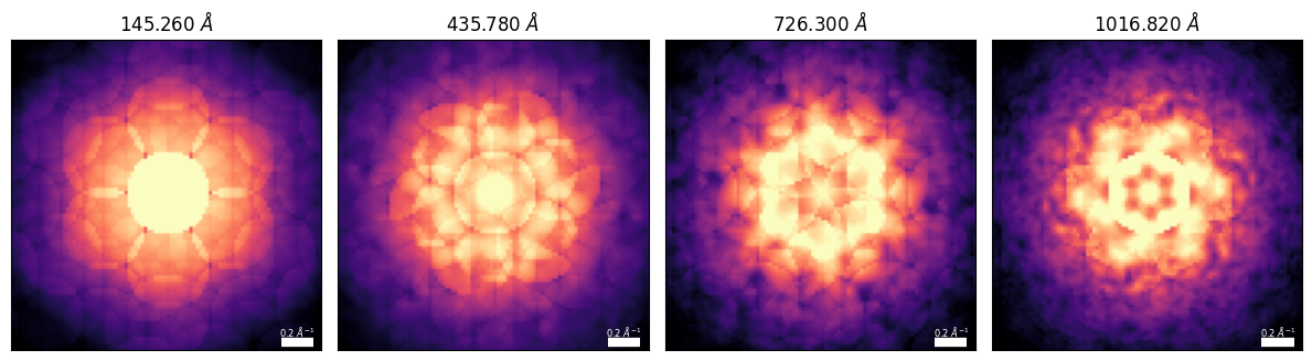
An even more robust related technique for estimating crystal thickness is to use a larger convergence angle to form a sub-Ångström focused probe, which is scanned across the sample. While each individual diffraction pattern is strongly-dependent on the position of the probe within the unit cell -- and thus our “independent” planewaves approach is invalid -- the technique averages across scan positions to produce a single PACBED pattern. This is mathematically equivalently to incoherently summing the contributions of independent tilted planewave calculations, so we can use the same formalism.
- De Graef, M. (2003). Introduction to Conventional Transmission Electron Microscopy. Cambridge University Press. 10.1017/cbo9780511615092

