STEM Measurements
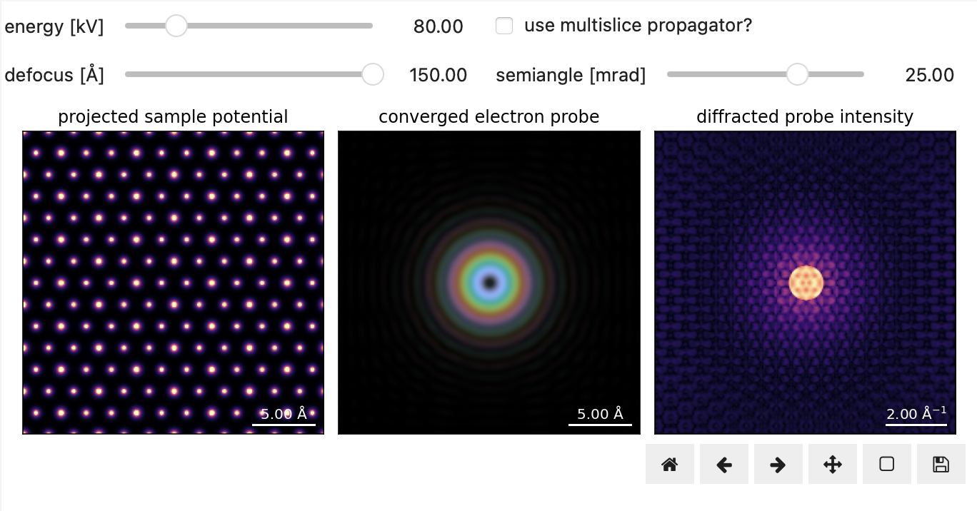
When an accelerated beam of electrons passes through a thin sample, the electron wavefunction is scattered due to interactions with the sample potential. Before describing the mathematics we will use the interactive widget below to obtain an intuition for the physics.
In the left panel of Figure 1.1, we are plotting the projected potential of a crystalline sample, specifically a thin film made up of 7 layers of gold viewed along the [111] zone-axis. In the middle panel of Figure 1.1 we are plotting the converged electron probe in real-space incident on the sample. Note the probe is complex-valued and here we are encoding the phase of the electron wavefunction using the hue channel. Finally, in the right panel of Figure 1.1 we are plotting the diffraction-space intensity of the probe after it has interacted with the sample. Note that the probe wavefunction is complex-valued, but we only plot its amplitude to highlight the limitation of current detectors in collecting the phase of the electron wavefunction.
The STEM techniques we will explore today such as bright-field (BF) STEM, dark-field (DF) STEM, differential phase contrast (DPC), or ptychography all share the same objective: namely to obtain robust estimates of the sample potential (left panel of Figure 1.1) using a set of diffraction intensities (right panel of Figure 1.1).


