Research
Comparing conventional ADF-STEM and 4DSTEM.
Scanning transmission electron microscopy (STEM) has become an essential tool for materials science research, where it has been applied to atomic-scale imaging, diffraction, spectroscopy, and 3D tomography of many materials. In conventional STEM imaging, we scan a converged electron probe in a 2D grid over the sample, recording 1-5 intensity values from detectors which count the electrons scattered over a large angular range. Complex electron diffraction patterns which encode a lot of atomic-scale sample information are therefore reduced to only a few measurement values in conventional STEM imaging.
However, we now have direct electron detectors which can operate at speeds up to 120,000 frames / second. These detectors allow us to record a full 2D image of the diffracted electron beam over a 2D grid of probe positions, generated a 4D dataset. We therefore coined the term four-dimensional scanning transmission electron microscopy (4DSTEM) to describe this family of experiments.
Our group has developed many kinds of 4DSTEM experiments, including nanobeam orientation and phase mapping, inversion of multiple scattering with physics and machine learning approaches, ptychographic imaging, ptychographic atomic electron tomography, and many others.
- (2023) Review of STEM in materials science
- (2021) 4DSTEM of beam-sensitive Materials
- (2019) Review of 4DSTEM
Analysis with py4DSTEM

4DSTEM experiments produce prodigious amounts of data - potentially millions of diffraction pattern images, each with tens of thousands of pixels. We have developed robust and efficient algorithms to analyze these huge 4DSTEM datasets, primarily implemented into open-source py4DSTEM python package developed by our group for analysis of 4DSTEM data. py4DSTEM provides researchers with a powerful, flexible, and user-friendly toolkit for processing and interpreting large-scale 4DSTEM data. The code supports a wide range of functionalities, including:
nanobeam crystalline diffraction data
- diffraction pattern indexing for orientation and phase mapping
- strain mapping
- structure classification
nanobeam amorphous diffraction data
- pair distribution function (PDF) mapping
- fluctuation electron microscopy (FEM)
- strain mapping
phase contrast STEM
- center of mass-differential phase contrast (CoM-DPC)
- parallax or tilt-corrected bright field imaging
- ptychography
- mutlislice ptychography
- joint ptychography-tomography
ML Inversion of Multiple Scattering
On of the most powerful aspects of electron microscopy is that electrons interact so strongly with matter - approximately an order of magnitude more strongly than photons! However, this strong interaction means that we need to make our samples extremely thin, thousands of times thinner than the diameter of a human hair. Ideally, we make samples so thin that most electrons scatter only a single time when passing through the material; however many samples are either too thick or contain heavy elements, and thus scatter the electron beam multiple times. This multiple scattering creates complex nonlinear contrast in our measured diffraction patterns, which cannot be analyzed with conventional analysis methods.
Our group has devised a way to overcome the limitations of multiple scattering in crystalline samples - we use deep learning methods to predict the single-scattering signal from diffraction patterns which contain strong multiple scattering. This allows us to analyze much thicker samples with electron microscopy, and to measure material structure and properties much more accurately.
ML Characterization of Disordered Materials
Disordered nanocrystalline silicon.
In the previous section, we saw how to invert multiple scattering signals from crystalline materials. But what about non-crystalline materials? Many important technological materials are highly disordered, including many functional oxides, silicate glasses, liquid or amorphous electrolytes, soft matter such as polymers, and many others. We are currently working to generalize our inversion methods to work on all materials, from fully disordered random liquids to highly ordered crystalline materials.
STEM Probe Wavefunction Control

Most STEM experiments use a very simple electron probe; a metal place with a circular hole is placed in the condenser aperture, which forms the the STEM probe in the far field. Our group has designed many custom STEM wavefunctions by placing patterned structures or devices into the probe-forming aperture. This allows us to design many different optical imaging considitions which module both the phase (the relative position of electron wavefronts) and amplitude (the number of incoming electrons at each angle) of the electron wave.
Phase Plates

In light optics, we have can control the shape of a light wave packet using a very large number of optical elements. However, in electron microscopy we have traditionally been limited to only two beam configurations: plane wave (or parallel) illumination, or converged beams formed from a circular aperture (the Airy disk function on the sample surface). In most TEMs, we can only modify converged electron beams by changing the defocus or the aperture size.
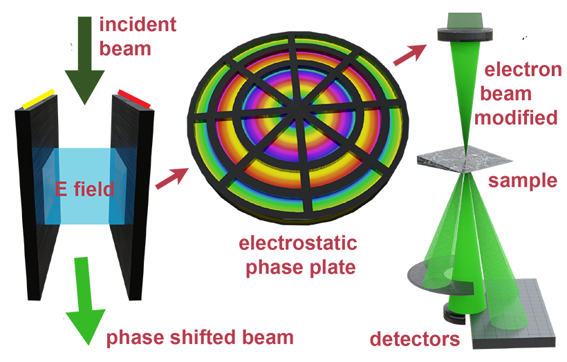
Our group has designed various phase plates which sit in the probe-forming aperture of TEM. These include passive phase plates used to enhance contrast, for example using our MIDI-STEM method. More recenlty we have designed active apertures which use electrostatic fields to modify the beam as shown in the above figure. These phase plates have a variety of uses, including potentially aberration correction.
Amplitude Plates

As we saw above, diffraction patterns from crystalline materials which contain multiple scattering are difficult to analyze. We have devised another 4DSTEM method to extract signals such as orientation or deformation strain - we insert patterned membranes into the probe-forming apertures. By stamping “bullseye” patterns into each diffracted probe, we allow our analysis software to extract material properties with much higher accuracy. See our paper patterned probes for high precision 4D-STEM bragg measurements for more information.
Atomic Electron Tomography
4DSTEM Ptychography

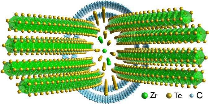
ZrTe nanowire encapsulated in double-walled carbon nanotube solved with PAET, from Pelz et al. (2023).
Our group pioneered the development of ptychographic atomic electron tomography, where we combine ptychographic imaging with AET. This approach significantly enhances the precision and sensitivity of atomic structure determination, enabling the visualization of complex nanostructures, including light elements. PAET has the potential to significantly expand the range of nanostructures that can be resolved in 3D at atomic resolution, and provide deeper insights into the atomic-scale underpinnings of material properties
- (2015) 3D positions of individual atoms in materials revealed by electron tomography
- (2017) Deciphering chemical order/disorder and material properties at the single-atom level
- (2019) Observing crystal nucleation in four dimensions using AET
- (2023) Solving complex nanostructures with PAET
- (2024) Atomic-scale identification of active sites of oxygen reduction nanocatalysts
ADF-STEM

Atomic electron tomography (AET) reconstructs the three-dimensional structures of materials at atomic resolution. By recording atomic-resolution images from many projection directions and then using tomographic reconstruction algorithms, we can use AET to map the 3D positions and species of atoms within complex nanostructures. This method is invaluable for studying defects, interfaces, and other structural intricacies in materials that influence their properties. AET has transformative applications in materials science, catalysis, and nanotechnology, offering unprecedented insights into the atomic-scale architecture of advanced materials. ADF STEM is particularly useful for AET studies, as it provides approximately linear contrast over a wide range of sample thicknesses, and produces contrast which depends on the atomic species.
HRTEM Tomography
As powerful as ADF-STEM is for AET studies, it has some critical drawbacks: ADF produces little or no contrast for light elements including important species such as C, O, Li and H, and requires a large electron beam dose which may damage beam-sensitive samples. Plane wave HRTEM imaging offers an alternative to STEM. Phase contrast HRTEM is very dose-efficient, and produces contrast for all atomic species. This is why HRTEM is the method of choice for imaging biological samples at high resolution. The problem with HRTEM is that it produces complex non-linear contrast, especially for thicker or strongly-scattering samples. In order to use it for AET, we have developed inverse multislice algorithms in collaboration with Laura Waller at UC Berkeley. We have collaborated with Michael Whittaker at Berkeley Lab to apply this method to solve the 3D structure of clay layers frozen in vitreous ice, even managing to find asymmetric ion concentrations which depend on the curvature of these sheets.
Data Analysis for Materials Characterization Science
Atomic Resolution Imaging
Scanning Probe Drift Correction
Analytical STEM is powerful because we can focus the electron beam down to a tiny spot, scanning it over the sample surface and recording various characterization signals. But this means that we record data sequentially; during the scanning time, the sample can move with respect to the beam due to mechanical or thermal motion, or the beam can cause charging which can cause the beam to move or even jump from the desired position. These sample drift artifacts can affect the accuracy of our measurements. What can we do to fix these artifacts?
The answer: use drift correction algorithms! We have developed a highly accurate method to correct STEM and SPM drift artifacts by combining multiple scans recorded at different scanning directions. This method works essentially by using the more accurate fast scan directions from each scan to measure and correct drift in the slow scan direction. We also took inspiration from tomographic reconstruction algorithms and developed a unique way to combine the data from different scan directions which reduces or even eliminates artifacts from the slow scan directions.
There are some commercial programs which fix sample drift. We have chosen instead to release our software freely to the research community. You can find the Matlab implementation of our algorithm on the github repo.
Quantum Mechanical Scattering Simulations
One of the most powerful tools for designing TEM experiments, data analysis, and hypothesis testing are TEM simulation algorithms. Our group has used, developed, and implemented many of these algorithms.
The PRISM Algorithm
The most commonly used algorithm for atomic resolution TEM and STEM simulation is the multislice method. In this method, we solve the Schrodinger equation using a split-step algorithm. We first divide up the samples into thin slices, define the initial wavefunction, and then alternate calculating scattering through each slice (the transmission operator) and then compute the wave evolution to the next slice (the propagation operator). We repeat these steps until the wavefunction reaches the bottom of the sample, and then compute the microscope transfer function and detector signal(s).
The multislice algorithm is powerful and works amazingly well for TEM experiments where we only need to calculate the scattering from one initial wavefunction. STEM is another matter however; each STEM probe position requires a unique calculation, creating potentially millions of unique calculations for large scan sizes. This can require unreasonably long calculation times. To address this issue, Colin developed the PRISM algorithm. PRISM can speed up STEM simulations by a ratio of to for an interpolation factor , which has typical values of 2-10, with a negligible loss in accuracy. This speedup can potentially be orders of magnitude for large scan sizes, and could be many many orders for inelastic scattering calculations.
We have extended this method using the partitioned PRISM algorithm which can provide even higher speedups at some cost to accuracy. Another group, inspired by the PRISM method, has developed the related Lattice Multislice Algorithm. PRISM has been implemented in our group’s Prismatic simulation code, and the all-python abTEM simulation code.
py4DSTEM Diffraction Simulations
- Ophus, C. (2023). Quantitative Scanning Transmission Electron Microscopy for Materials Science: Imaging, Diffraction, Spectroscopy, and Tomography. Annual Review of Materials Research, 53(1), 105–141. 10.1146/annurev-matsci-080921-092646
- Bustillo, K. C., Zeltmann, S. E., Chen, M., Donohue, J., Ciston, J., Ophus, C., & Minor, A. M. (2021). 4D-STEM of Beam-Sensitive Materials. Accounts of Chemical Research, 54(11), 2543–2551. 10.1021/acs.accounts.1c00073
- Ophus, C. (2019). Four-Dimensional Scanning Transmission Electron Microscopy (4D-STEM): From Scanning Nanodiffraction to Ptychography and Beyond. Microscopy and Microanalysis, 25(3), 563–582. 10.1017/s1431927619000497
- Ophus, C., Zeltmann, S. E., Bruefach, A., Rakowski, A., Savitzky, B. H., Minor, A. M., & Scott, M. C. (2022). Automated Crystal Orientation Mapping in py4DSTEM using Sparse Correlation Matching. Microscopy and Microanalysis, 28(2), 390–403. 10.1017/s1431927622000101
- Pekin, T. C., Gammer, C., Ciston, J., Minor, A. M., & Ophus, C. (2017). Optimizing disk registration algorithms for nanobeam electron diffraction strain mapping. Ultramicroscopy, 176, 170–176. 10.1016/j.ultramic.2016.12.021
- Kennedy, E., Reynolds, N., Rangel DaCosta, L., Hellman, F., Ophus, C., & Scott, M. C. (2020). Tilted fluctuation electron microscopy. Applied Physics Letters, 117(9). 10.1063/5.0015532
- Ribet, S. M., Varnavides, G., Pedroso, C. C. S., Cohen, B. E., Ercius, P., Scott, M. C., & Ophus, C. (2024). Uncovering the three-dimensional structure of upconverting core–shell nanoparticles with multislice electron ptychography. Applied Physics Letters, 124(24). 10.1063/5.0206814
- Munshi, J., Rakowski, A., Savitzky, B. H., Zeltmann, S. E., Ciston, J., Henderson, M., Cholia, S., Minor, A. M., Chan, M. K. Y., & Ophus, C. (2022). Disentangling multiple scattering with deep learning: application to strain mapping from electron diffraction patterns. Npj Computational Materials, 8(1). 10.1038/s41524-022-00939-9
- Ophus, C., Ciston, J., Pierce, J., Harvey, T. R., Chess, J., McMorran, B. J., Czarnik, C., Rose, H. H., & Ercius, P. (2016). Efficient linear phase contrast in scanning transmission electron microscopy with matched illumination and detector interferometry. Nature Communications, 7(1). 10.1038/ncomms10719
- Ribet, S. M., Zeltmann, S. E., Bustillo, K. C., Dhall, R., Denes, P., Minor, A. M., dos Reis, R., Dravid, V. P., & Ophus, C. (2023). Design of Electrostatic Aberration Correctors for Scanning Transmission Electron Microscopy. Microscopy and Microanalysis, 29(6), 1950–1960. 10.1093/micmic/ozad111
- Zeltmann, S. E., Müller, A., Bustillo, K. C., Savitzky, B., Hughes, L., Minor, A. M., & Ophus, C. (2020). Patterned probes for high precision 4D-STEM bragg measurements. Ultramicroscopy, 209, 112890. 10.1016/j.ultramic.2019.112890
- Pelz, P. M., Griffin, S. M., Stonemeyer, S., Popple, D., DeVyldere, H., Ercius, P., Zettl, A., Scott, M. C., & Ophus, C. (2023). Solving complex nanostructures with ptychographic atomic electron tomography. Nature Communications, 14(1). 10.1038/s41467-023-43634-z
- Xu, R., Chen, C.-C., Wu, L., Scott, M. C., Theis, W., Ophus, C., Bartels, M., Yang, Y., Ramezani-Dakhel, H., Sawaya, M. R., Heinz, H., Marks, L. D., Ercius, P., & Miao, J. (2015). Three-dimensional coordinates of individual atoms in materials revealed by electron tomography. Nature Materials, 14(11), 1099–1103. 10.1038/nmat4426
- Yang, Y., Chen, C.-C., Scott, M. C., Ophus, C., Xu, R., Pryor, A., Wu, L., Sun, F., Theis, W., Zhou, J., Eisenbach, M., Kent, P. R. C., Sabirianov, R. F., Zeng, H., Ercius, P., & Miao, J. (2017). Deciphering chemical order/disorder and material properties at the single-atom level. Nature, 542(7639), 75–79. 10.1038/nature21042
- Zhou, J., Yang, Y., Yang, Y., Kim, D. S., Yuan, A., Tian, X., Ophus, C., Sun, F., Schmid, A. K., Nathanson, M., Heinz, H., An, Q., Zeng, H., Ercius, P., & Miao, J. (2019). Observing crystal nucleation in four dimensions using atomic electron tomography. Nature, 570(7762), 500–503. 10.1038/s41586-019-1317-x

